ECoVEM project brings together VET centres, polytechnics, industrial associations, social partners to establish European Cooperation platform of Vocational Excellence in Microelectronics to tackle the challenges of: digitalisation, artificial intelligence, green technologies, gender equality and technology, integration of migrants.
ECoVEM builds on and complements the strengths of national VET systems in countries with more advanced VET and supports the not so advanced regions to achieve VET excellence. ECoVEM implements innovative instructional approaches towards life-long capacity to self-regulate learning, hard skills and soft skills using the ecosystems-based theoretical models and performance support systems. The most relevant processes related to microelectronics technology are design and manufacturing.
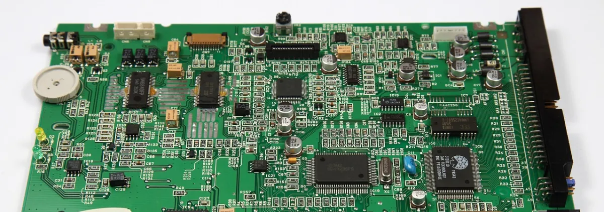
The entire process of creating a silicon wafer with working chips consists of thousands of steps and can take more than three months from design to production. The design process includes all aspects of microelectronics design, from the development of novel designs to research into design tools, processes, and design automation. The manufacturing process involves not only the most common manufacturing steps like deposition, photoresist, lithography, etch, ionization, and packaging, but also measurement and inspection, testing, and much more.
This course introduces the microelectronics manufacturing processes commonly used in chip mass production, from the fabrication of a silicon wafer to the packaging process, and focuses on the complex high-technology machinery needed to achieve work in this nanoworld. Students will learn the state of the art and future challenges in manufacturing and measurement. Theoretical and practical aspects will be introduced to get a complete technical overview of the manufacturing processes.
Resource available: course